English
  日本語
日本語  한국어
한국어  français
  Deutsch
  Español
  italiano
  русский
  português
  العربية
  ไทย
ไทย 
In today's rapidly advancing world, electronics play a pivotal role in our daily lives. From smartphones to home appliances, almost every aspect of our life is touched by the wonders of technology. However, have you ever wondered how these electronics come to life? Behind the scenes lies a complex process called PCB fabrication. At the heart of this process is a crucial component known as lithography lenses.
Lithography lenses, also known as photomask or masking lenses, are essential in the creation of printed circuit boards (PCBs). These lenses are used to transfer the intricate patterns and designs onto the surface of the PCB. Without them, the production of complex and high-density electronic circuits would be nearly impossible.
The process begins with the creation of a photomask, which contains the desired circuit pattern. This mask is positioned in front of the lithography lens. A light source projects the pattern through the lens, which then focuses the light onto the surface of the PCB. The areas exposed to light undergo a chemical transformation, leading to the formation of conductive paths and insulating regions on the board.
One key aspect of lithography lenses is the resolution they provide. Resolution refers to the ability of the lens to accurately reproduce the fine details of the circuit pattern. As technology advances, the demand for higher resolution lenses increases. The higher the resolution, the smaller the features that can be created on the PCB, allowing for increased circuit complexity and miniaturization.
To achieve higher resolution, manufacturers have developed different lens types, such as immersion lenses and advanced lens materials. Immersion lenses use a liquid medium between the lens and the photomask, enabling the reduction of the wavelength of light passing through it. This reduction in wavelength improves the resolution of the lens, allowing for the creation of finer circuit patterns.
Furthermore, advancements in lens materials have also played a significant role in improving lithography processes. Lenses made from materials with high refractive indices, such as calcium fluoride and synthetic quartz, have better light transmission properties. This results in improved image quality and enhanced resolution.
In addition to resolution, other factors such as depth of focus, aberrations, and lens quality are crucial in lithography lenses. Depth of focus refers to the range of distances that the lens can focus on while maintaining acceptable image quality. Aberrations, on the other hand, are distortions or imperfections in the lens, affecting the quality of the projected image. Therefore, manufacturers strive to produce high-quality lithography lenses with minimal aberrations to ensure precise circuit pattern replication.
In conclusion, lithography lenses are the unsung heroes in the world of electronics and PCB fabrication. Without them, the intricate circuit patterns that power our daily lives would not exist. As technology continues to evolve, the demand for higher resolution and improved lithography processes will only increase. Through innovations in lens materials and design, manufacturers are pushing the limits of what is possible in the world of electronics. So, the next time you pick up your smartphone or use any electronic device, remember the invaluable contribution of lithography lenses in bringing them to life.
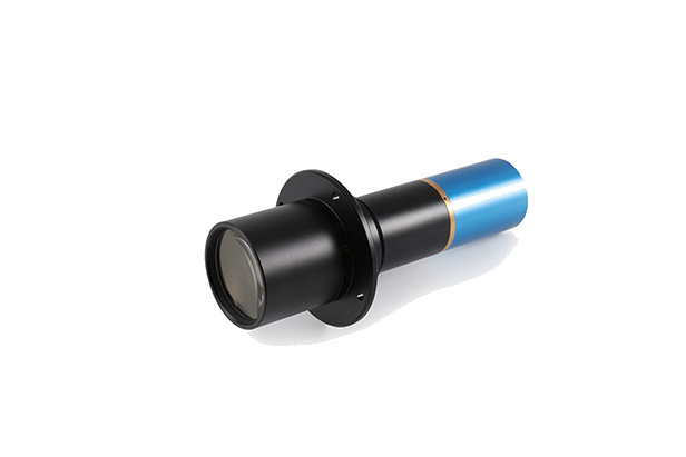
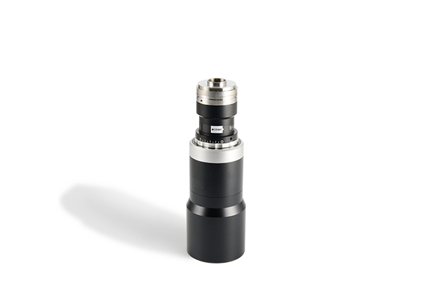
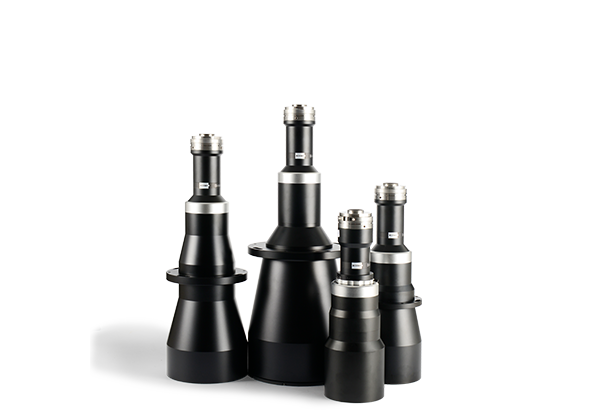
Related Machine Vision Telecentric Lens Products