English
  日本語
日本語  한국어
한국어  français
  Deutsch
  Español
  italiano
  русский
  português
  العربية
  ไทย
ไทย 
With the further development of machine vision technology, various types of machine vision devices are increasingly being used in various industries.
Among them, the electronic manufacturing industry and the semiconductor industry are the fields where machine vision is widely applied. In the electronic manufacturing industry, machine vision systems are applied in every aspect of electronic manufacturing, from small components such as capacitors and connectors to large components such as mobile phone keyboards, PC motherboards, and hard drives.
The semiconductor industry is typified by upstream wafer processing and manufacturing, cutting, printing, and repairing of circuit boards, all of which depend on high-precision machine vision to guide and locate moving parts.
Machine vision is mainly used in the electronic manufacturing field to guide robots in high-precision PCB positioning and SMT component placement. According to data, the electronics industry is the industry that uses machine vision measurement systems most widely, accounting for about 50% of the demand for machine vision. It is also used for defect detection, hole alignment, silk screen quality inspection, SPI solder paste inspection, reflow soldering and wave soldering, surface quality inspection of electronic components, and marking inspection in various production and assembly equipment.
In general, conventional online visual inspection applications place industrial cameras on the circuit board to obtain images of the printing position and send the relevant images to the processing system of the visual inspection device. The software then analyzes the image. The software compares the obtained image with the reference image stored in the device memory at the same position.
In this way, the machine vision inspection system can determine whether more or less solder paste is being applied. The system can also show whether the solder paste on the solder pad is aligned. It is possible to detect whether there is excess solder paste forming a "bridge" between two solder pads.
The work of detecting the gap in the print template is also in the same format. When excessive solder paste accumulates on the surface of the printing template, a visual inspection system can be used to detect whether the gap is blocked by the solder paste or whether there is a tailing phenomenon.
When a defect is found, the equipment can immediately automatically request a series of cleanings, or warn the operator that there is a problem and that maintenance is required. Checking the print template can also provide very useful data to the user about print quality and consistency.
In addition, a key function of advanced online visual inspection systems which includes a telecentric objective is the ability to detect differences in high-reflective PCB circuit boards and solder pad surfaces under uneven lighting conditions or due to dry solder paste structures. For example, HASL circuit boards typically have characteristics such as roughness, surface contour variability, and reflectivity. Proper lighting also plays a very important role in obtaining the highest quality images.
The light must be able to "target" the circuit board's base and solder pad, and then convert other difficult-to-perceive functions into clear and recognizable shapes. In this way, the potential can be fully realized using a visual software rule system.
In some special cases, the machine vision system can be used to detect the height or volume of solder paste on the solder pad. Sometimes, it may only use an offline visual inspection system to perform these operations. Using this procedure means forming a corresponding stack in a given print template to determine whether there is a lack of solder paste on the same solder pad.
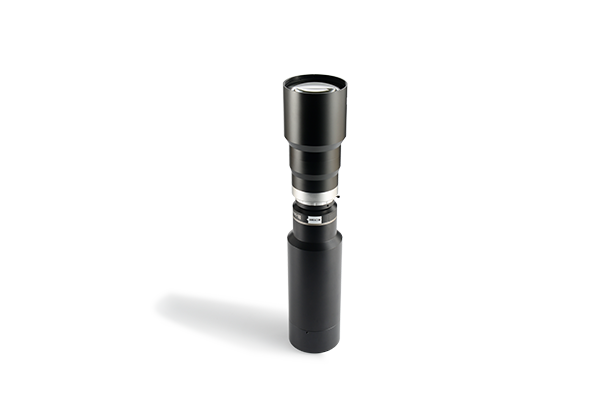
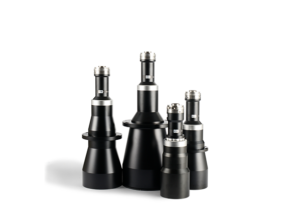
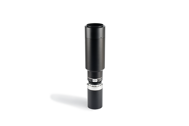
Related Machine Vision Telecentric Lens Products