
Leave Your Message
High-resolution, low-distortion telecentric lenses designed to identify micro-cracks and structural flaws in photovoltaic manufacturing.


Why advanced optical inspection is critical in modern photovoltaic manufacturing processes.
In the global drive toward clean, renewable energy, the photovoltaic (PV) industry is scaling production speeds and wafer sizes while simultaneously reducing wafer thicknesses. Modern solar cells, often as thin as 130 to 170 micrometers, are highly fragile. Throughout the manufacturing cycle—encompassing ingot slicing, wafering, cell processing, stringing, and module lamination—silicon wafers are subjected to intense mechanical handling and thermal stresses.
These stresses inevitably trigger the formation of micro-cracks, edge chips, finger breaks, and crystal dislocations. Micro-cracks are particularly problematic. Unlike surface scratches, micro-cracks are often buried deep within the silicon substrate, invisible to the naked eye and traditional imaging systems. If left undetected, environmental stresses (such as thermal expansion, wind loads, and snow accumulation) will cause these micro-cracks to propagate over time. The consequences are severe: local hotspots, localized power loss, accelerated cell degradation, and in extreme cases, thermal runaway or complete module failure in the field.
"According to industry statistics, optical defects and micro-cracks account for over 45% of early-stage solar module failures. Implementing high-precision, automated optical inspection (AOI) utilizing telecentric zoom lenses is no longer optional—it is a critical prerequisite for quality assurance and brand integrity."
Standard machine vision lenses suffer from perspective errors, distortion, and variation in magnification when the object distance shifts. In high-speed solar cell production lines, minor vibrations, belt movements, or variations in wafer flatness can alter the working distance. If a standard lens is used, this change in distance alters the image size, leading to false defect classifications or missed micro-cracks.
A telecentric zoom lens solves these challenges through unique optical properties:
How telecentric imaging systems are deployed at critical stages of the photovoltaic manufacturing workflow.
Immediately after the wire-sawing process, silicon wafers must be inspected for micro-cracks, thickness variations, and saw marks. Telecentric lenses paired with high-resolution line-scan cameras capture the precise geometry of the wafer edges. The zero-distortion profile of the lens ensures that micro-chips along the wafer perimeter—which are the primary nucleation sites for future cracks—are identified with micrometer-level accuracy before the wafer moves to the chemical etching stage.
EL and PL imaging are the most reliable methods for detecting internal defects in solar cells. In EL inspection, an electric current is passed through the cell, causing it to emit near-infrared (NIR) light. In PL inspection, external laser light is used to excite the silicon, generating luminescence without contact.
Because the emitted light is extremely weak and concentrated in the 900nm to 1100nm spectrum, the optical system must feature high light transmission and optimal sensor integration. Telecentric lenses optimized for NIR and Short-Wave Infrared (SWIR) spectra gather maximum light while keeping the image completely flat. This enables the machine vision software to accurately map micro-cracks, dark spots, and crystal boundary defects across the entire wafer surface.
To maximize efficiency, modern solar cells employ multi-busbar designs with ultra-thin ribbon wires. The alignment and soldering quality of these busbars must be checked in real-time. Parallax errors from standard lenses can misrepresent the position of the busbars relative to the grid lines. Telecentric zoom lenses provide the exact coordinate measurement needed to guide robotic positioning systems and inspect solder joints, ensuring optimal electrical conductivity and mechanical stability.
The technological trajectory of optical inspection systems in the global solar energy market.
As solar cell sizes transition to G12 (210mm x 210mm) and beyond, imaging systems require larger sensors (such as 67mm or 82mm line scan sensors) to cover the entire area without stitching images. This requires telecentric lenses with large image circles that can maintain high resolution and contrast from the center to the very edge of the sensor.
Modern PV inspection machines are rapidly adopting AI-driven defect classification. AI algorithms perform best when fed with clean, standardized, and distortion-free images. Telecentric lenses act as the perfect optical front-end, providing consistent raw data that minimizes false positives and enhances the training efficiency of deep neural networks.
Newer solar cell architectures, such as TOPCon (Tunnel Oxide Passivated Contact) and HJT (Heterojunction Technology), require inspection at deeper infrared wavelengths. The future of telecentric zoom lenses lies in multispectral coatings that span from visible light to SWIR (900nm - 1700nm), allowing a single optical setup to perform multiple inspection tasks simultaneously.
Leading the Industry in Telecentric Optical Technology and Precision Lens Design
From manufacturing to creation, we are on the way.
Canrill Optics, established in 2009, is the first one to focus on the manufacturing & marketing of telecentric lens and telecentric lens design in China, and the only one to build the complete supply chain with our own mechanical factory and optical factory in industry lens all over the world.
Over the years, as a custom lens manufacturer, Canrill lens has been upgraded four generations with advanced technology and performance, earned the trust from worldwide clients, and have successfully made cooperation with world-famous brands, like Samsung, Apple, LG, Huawei, Han’s Laser, TSMC, etc.

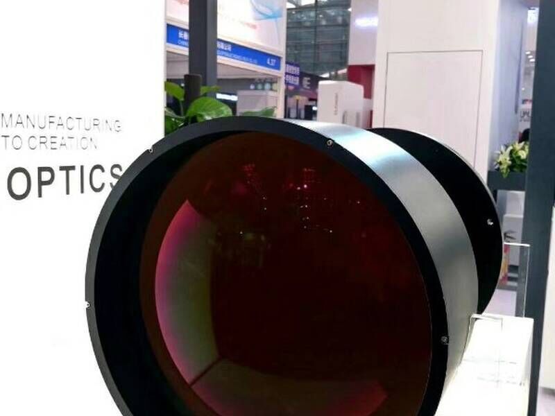
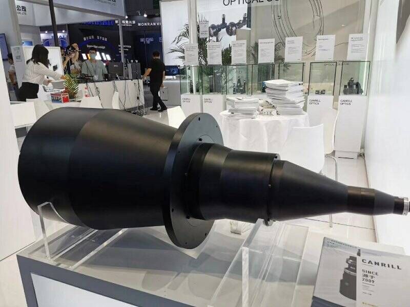
The Optical Experts and Visionaries Driving Innovation at Canrill Optics

Since founding Canrill in 2009, Simon has been focused on building the world leading manufacturer of telecentric lenses. Under Simon's leadership, Canrill has grown into a 100+ person company which is renowned in both China and overseas.

Senior optical designer, with 10+ years' experience in the design and inspection of telecentric lens and lights.

15+ years' experience in the mechanical design, ensuring precision engineering for all custom optical assemblies.
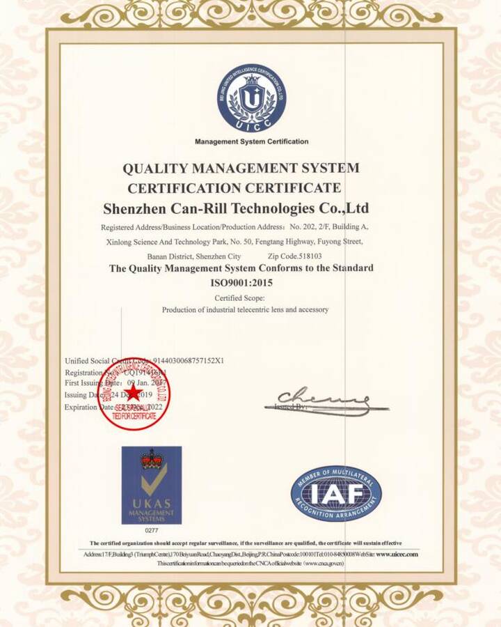 Canrill ISO 9001
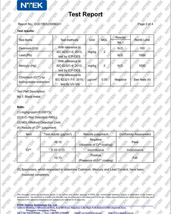 RoHS Certificate 1
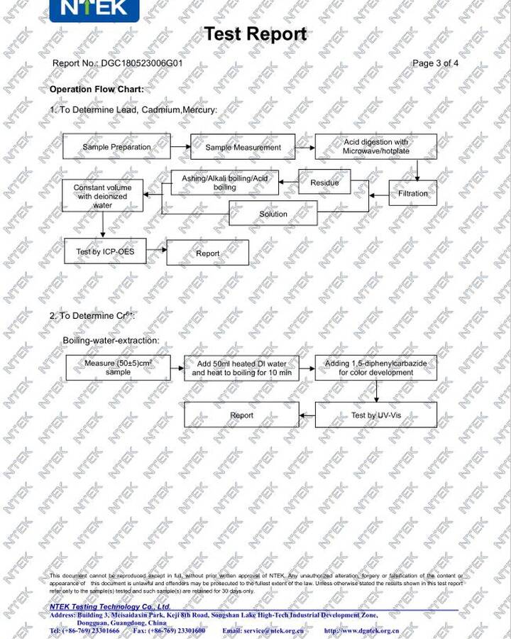 RoHS Certificate 2
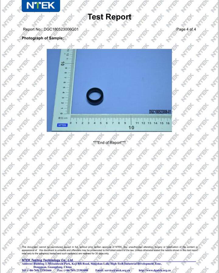 RoHS Certificate 3
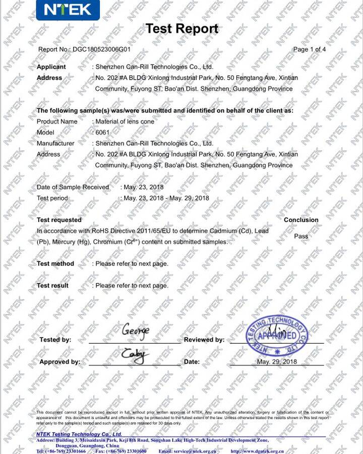 RoHS Certificate 4
Explore our full range of industrial lenses optimized for high-speed, high-precision photovoltaic wafer and cell inspection.


