
Leave Your Message


In the rapidly evolving landscape of electronics manufacturing, the demand for high-density, multi-layered, and ultra-miniaturized Printed Circuit Boards (PCBs) is at an all-time high. Modern PCBs house thousands of micro-components, fine-pitch traces, and complex solder configurations. As component spacing shrinks to the sub-millimeter level, conventional imaging systems struggle to deliver the precision required for automated quality inspection. This is where telecentric camera systems and specialized lenses have become indispensable.
Unlike standard lenses, which suffer from perspective errors and magnification shifts when the distance to the target changes, a telecentric lens maintains constant magnification across the entire depth of field. This unique optical property ensures that three-dimensional PCB features—such as tall capacitors, IC packages, and solder joints—are captured without parallax distortion. By eliminating perspective error, telecentric camera systems provide Automated Optical Inspection (AOI) machines with the precise dimensional accuracy needed to detect critical defects, including solder bridging, missing components, component misalignment, and hairline trace cracks.
The global market for PCB defect detection is undergoing a profound technological shift. Driven by the expansion of 5G, consumer electronics, electric vehicles (EVs), and aerospace technologies, the cost of component failure has skyrocketed. A single defective solder joint on an automotive ADAS control board or a medical device PCB can lead to catastrophic system failures. Consequently, manufacturers are transitioning from random sampling to 100% automated inline inspection.
From a commercial perspective, integrating high-performance telecentric camera setups directly impacts the bottom line by reducing the False Call Rate (FCR) and the Escape Rate. A high FCR forces manufacturers to dedicate excessive human labor to manual re-inspection, slowing down production lines. Conversely, a high Escape Rate allows defective boards to reach final assembly, leading to costly warranty claims and brand damage. By delivering pixel-perfect, orthographic images, telecentric optics provide the clean data feeds that modern machine learning and AI-based inspection algorithms require to classify defects accurately.
Inspecting solder fillets requires capturing precise 3D profiles. Telecentric cameras prevent the reflections and shadows of neighboring tall components from obscuring the solder joints, ensuring accurate volume and height measurements.
Ball Grid Array (BGA) and Quad Flat No-leads (QFN) components must sit perfectly flat. Telecentric lenses verify component coplanarity across the entire PCB, identifying minute tilts or lift-offs that lead to open circuits.
For high-density interconnect (HDI) substrates, track width and spacing must be measured with sub-micron accuracy. The ultra-low distortion of bi-telecentric lenses guarantees consistent edge detection across the entire sensor area.
As sensor technology advances, telecentric lenses are adapting to support larger formats and higher pixel densities. The integration of 151-megapixel sensors and 12K line scan cameras allows AOI systems to inspect massive PCB panels in a single pass without sacrificing spatial resolution. Furthermore, the combination of telecentric optics with multi-angle coaxial LED illumination helps eliminate specular reflections from metallic solder joints, highlighting surface defects with exceptional contrast.
Another significant trend is the rise of 3D AOI systems. By combining structured light projection with telecentric cameras, these systems reconstruct a complete 3D height map of the PCB. The constant magnification of the telecentric lens ensures that the projected fringe patterns are mapped accurately to the physical coordinates of the board, allowing for precise volumetric measurements of solder paste deposits.
Manufacturing optical systems capable of sub-micron precision requires an uncompromising commitment to quality control. At Canrill Optics, every step of our design and production process is engineered to guarantee that our telecentric lenses perform flawlessly under the rigorous conditions of 24/7 industrial PCB inspection lines.
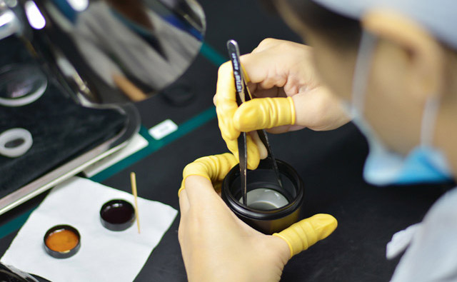
ISO9001:2015 Certified Production Line
Canrill Quality Management System conforms to the standard of ISO9001:2015 in the production of industrial telecentric lenses and accessories. Our Quality Department consists of 13 experienced specialists, representing more than 13% of the total personnel at Canrill. This high ratio underscores the critical importance we place on quality assurance across our entire manufacturing workflow.
Our Quality Department operates across four specialized, independent branches to ensure objective verification: IQC (Incoming Quality Control), IPQC (Input Process Quality Control), QA (Quality Assurance), and OQC (Outgoing Quality Control). Together, they enforce a rigorous 7-stage quality pipeline:
Verification of model names, configurations, and raw material quantities against design specifications.
Detailed evaluation of component appearance, dimensional tolerance, surface oxidation, and optical material properties.
Segregation and labeling of qualified materials from unqualified ones, maintaining clean storage conditions.
Strict assembly following technical drawings and BOM lists, ensuring no missing screws, precise glue application, and perfect mechanical fit.
Comprehensive optical verification: testing image clarity, working distance, telecentricity, optical distortion, and resolving power.
Final inspection of lens appearance (ensuring zero scratches, aberrations, white dots, or dust), checking that the lens cone gap is under 0.1mm, verifying structural integrity, and confirming the correct attachment of serial number stickers.
Verification of box contents, packaging robustness, desiccant inclusion, certificates of qualification, and related accessories before shipment.


