
Leave Your Message
Engineered specifically for automated defect mapping, solder paste inspection, and component alignment.


In the contemporary electronics manufacturing industry, Printed Circuit Boards (PCBs) serve as the foundational nervous system for everything from consumer devices to automotive control units and aerospace instrumentation. As consumer electronics demand smaller form factors and automotive sectors push towards electrification, the complexity of PCBs has grown exponentially. High-Density Interconnect (HDI) boards, flexible circuits, and multi-layered configurations now feature trace widths and spaces measured in microns.
This miniaturization has made manual optical inspection obsolete. The global market for automated PCB defect detection is undergoing a massive shift, driven by the requirement for zero-defect reliability. In industries like electric vehicles (EVs) and medical electronics, a single faulty solder joint or micro-crack in a trace can lead to catastrophic system failure. Consequently, 100% inline Automated Optical Inspection (AOI) and 3D Solder Paste Inspection (SPI) have become mandatory standards rather than optional quality checkpoints.
Telecentric optics ensure vertical views of tall components, preventing perspective shifts and false defect flags.
Uncompromising optical clarity designed to capture hairline fractures, bridge defects, and micro-via irregularities.
Ultra-low distortion profiles guarantee dimensional measurement accuracy across the entire field of view.
During the Surface Mount Technology (SMT) and assembly process, industrial camera lenses are deployed at multiple critical junctions. Understanding these application scenarios reveals why selecting the appropriate optical lens is paramount for machine vision integrators.
SPI systems are positioned directly after the solder paste printer. They measure the volume, area, height, and registration of the deposited solder paste before components are placed. Because solder paste deposit is a three-dimensional structure, standard entocentric lenses suffer from perspective distortion (parallax error) at the periphery of the field of view. By utilizing bi-telecentric lenses, SPI systems maintain constant magnification even if the board is slightly warped, ensuring highly accurate volumetric measurements.
Pre-reflow AOI verifies component presence, placement accuracy, and polarity. Post-reflow AOI inspects the quality of the solder joint after the board passes through the reflow oven. The challenges here are the varied heights of components (e.g., tall electrolytic capacitors next to flat chip resistors) and highly reflective solder surfaces. Industrial lenses with high depth of field (DOF) and low chromatic aberration are required to keep both the top of tall components and the solder pads in sharp focus, eliminating false failures in automated algorithms.
For advanced semiconductor substrates and HDI PCBs, traces are packed closely together. Lenses must resolve micro-vias (laser-drilled holes connecting layers) that are less than 50μm in diameter. This requires high-magnification, large-format telecentric lenses paired with high-resolution line scan or area scan sensors. These lenses must deliver flat-field imaging with zero vignetting to ensure consistent resolution from the center to the very edge of the sensor.
The future of PCB inspection is deeply intertwined with advancements in optoelectronics and software algorithms. We are witnessing several key trends:
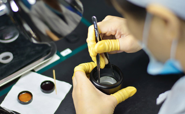
Canrill Quality Management System conforms to the standard of ISO9001:2015 in the production of industrial telecentric lens and accessory. Our Quality Dept consists of 13 experienced persons, representing more than 13% share of the total personnel in Canrill, showing the importance of quality in Canrill's whole system.
Our Quality Department operates across four specialized branches: IQC (Incoming Quality Control), IPQC (Input Process Quality Control), QA (Quality Assurance), and OQC (Outgoing Quality Control). Each branch works independently to guarantee the flawless optical and mechanical performance of every telecentric lens.
Appearance checks (no scratches, aberration, white dots, or dust), lens cone gaps < 0.1mm, no loose parts, proper labeling on both lens & box, accessory verification, desiccant, certificate of qualification, and coaxial light testing.
Strict verification of model name, technical specifications, and quantities against raw orders.
Comprehensive inspection of physical appearance, mechanical specification tolerance, surface oxidation, and raw material purity.
Clear segregation of qualified and unqualified materials, model and quantity logging, and secure packaging protection.
BOM list compliance, perfect cosmetic checks, strict assembly according to engineering drawings, ensuring no missing screws or glue.
Final check of shipment quantity, packaging appearance, stickers, accessories, and box durability.
Rigorous optical testing for clear imaging, absence of angle ambiguity, precise working distance validation, telecentricity verification, and distortion measurement.
High-performance industrial lenses designed for the most demanding PCB defect detection and metrology systems.

